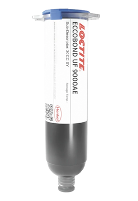
LOCTITE ECCOBOND UF 9000AE
Harmonization Code : 3506.91.90.99 | Prepared glues and other prepared adhesives, not elsewhere specified or included; products suitable for use as glues or adhesives, put up for retail sale as glues or adhesives, not exceeding a net weight of 1 kg ; Adhesives based on polymers of headings 3901 to 3913 or on rubber; Other ; Other
Main features
- Low die warpage
- Best large die underfill
- 260°C reflow capability for Pb- free, low-k applications
Product Description
LOCTITE® ECCOBOND UF 9000AE is a cutting-edge semiconductor capillary underfill designed specifically to meet the demands of next-generation flip-chip BGA (FCBGA) and high-density fan-out (HD-FO)/2.5D integrated advanced packaging designs. These technologies, critical for AI and high-performance computing (HPC) applications, feature large, high-density I/O die within expansive package dimensions, making warpage prevention and die protection crucial for long-term reliability.
LOCTITE® ECCOBOND UF 9000AE excels in this environment by offering robust protection against die warpage and cracking, which are common concerns due to the fine-pitch interconnects found on large die. This PFAS-free epoxy encapsulant boasts a fast flow rate, ensuring that it can fill gaps efficiently while maintaining the integrity of the delicate interconnects. Its high fracture toughness further enhances durability, ensuring that the die remains protected under various operational stresses.
Once fully cured, LOCTITE® ECCOBOND UF 9000AE forms a rigid, self-filleting protective seal that significantly improves the reliability of solder joints. This protective layer not only extends the electrical, thermal, and moisture resistance of the package but also helps to dissipate stress, thereby enhancing overall performance and longevity. The underfill’s low thermal expansion, fast capillary flow, and extended work-life make it an ideal solution for complex, high-density semiconductor packages, ensuring both comprehensive interconnect protection and high processability. It is the best underfill for large die sizes and flip chips applications with small gaps.
Applications
- Flip-Chip Ball Grid Array (BGA), Cu Pillar Package, and other high-density interconnect designs
Cure schedule
- 15 minute ramp to 100°C; 90 minute hold @ 100°C + 15 minute ramp from 100°C to 165°C; 2 hour hold @ 165°C
ECCOBOND UF9000AE
Loading pricing…
 Shipping in 28 days
 Shipping in 12 weeks
 Shipping in 25 days
Packaging
Technical Specifications
General Properties
Thermal Properties
Physical Properties
Additional Information
LOCTITE ECCOBOND UF 9000AE
LOCTITE ECCOBOND UF 9000AE is a black, heat-cure epoxy capillary underfill developed for large-die flip-chip BGA, Cu pillar, HD-FO and 2.5D advanced packaging. Its low CTE, fast capillary flow, low resin bleed out and self-filleting cured form are designed to support fine-pitch interconnect encapsulation, warpage control and package reliability in high-density AI and HPC package architectures.
Key liquid properties
These values describe the uncured product at the stated conditions. Capillary-flow behavior during dispensing should be evaluated with the intended package geometry and heated process conditions.
| Property | Typical value | Condition / context |
|---|---|---|
| Technology | Epoxy | TDS product description |
| Appearance | Black liquid | As supplied |
| Viscosity | 9,082 mPa s (cP) | Brookfield CP 51, 25 deg C, 5 rpm |
| Thixotropic index | 0.85 | 0.5/5 rpm |
| Specific gravity | 1.71 | 25 deg C |
| Pot life | 24 hr | 25 deg C |
| Average particle size | 1 um | As supplied |
| Maximum particle size | 5 um | As supplied |
| Shelf life | 180 days | Stored at -40 deg C |
Capillary underfill process guidance
Henkel recommends conditioning the material to room temperature before use, preheating the substrate for even under-die flow, controlling the dispense pattern and delay between passes, and completing the documented stepped heat cure. The recommended profile is a guideline and may require adjustment for the customer's equipment, oven loading and application.
Frozen storage and thawing controls
Store the unopened product in a dry location at an optimal storage temperature of -40 deg C. Storage above -15 deg C can adversely affect product properties. Once thawed to 25 deg C, do not re-freeze the material.
| Package format | Recommended thaw time |
|---|---|
| 10 cc syringe | 1 hr |
| 30 cc syringe | 1.5 hr |
| 55 cc syringe | 2 to 3 hr |
| 6 oz cartridge | 4 to 5 hr |
Thermomechanical properties
The cured property data below are typical reference values from the February 2024 TDS. Tg is reported by both DMA and TMA and should remain tied to the stated test method.
| Property | Typical value | Method / region |
|---|---|---|
| Coefficient of thermal expansion | 23 ppm/deg C | Below Tg |
| Coefficient of thermal expansion | 85 ppm/deg C | Above Tg |
| Glass transition temperature | 111 deg C | DMA |
| Glass transition temperature | 112 deg C | TMA |
| Storage modulus | 13,500 N/mm^2 | DMA at 25 deg C |
| Storage modulus | 136 N/mm^2 | DMA at 250 deg C |
Large-die flow and reliability evidence
Henkel positions UF 9000AE for highly integrated packages where complete interconnect coverage, low warpage propensity and crack resistance are important. The supplier attributes these characteristics to fast capillary flow, low CTE, low shrinkage and high fracture toughness.
| Evaluation | Conditions / scope | Supplier-reported result |
|---|---|---|
| Capillary-flow comparison | 40 mm x 40 mm die; internal testing versus previous-generation capillary underfills | 20% faster flow reported; result is die-size dependent. |
| Large-die validation | Die sizes up to 50 mm x 50 mm | Henkel reports product performance validated at this die size. |
| Large-package validation | Package bodies up to 110 mm x 110 mm | Henkel reports demonstrated effectiveness at this package size. |
| Fine-pitch encapsulation | 100 um I/O pitch and low gap heights >45 um | Low/no-voiding bump encapsulation reported in the product info sheet. |
| Reliability evaluation | MSL3a + 2,000 TCT-B cycles; 192 hr uHAST; 1,000 hr HTS at 150 deg C | Henkel reports good reliability across the listed evaluations. |
The comparative 20% flow result is explicitly die-size dependent. Reliability and package-level results should be evaluated against the intended package geometry, process conditions and customer qualification requirements.
Advanced-package application fit
The product is intended for semiconductor underfill and electronic encapsulation, with documented use contexts centered on large-die, high-density interconnect packages.
LOCTITE ECCOBOND UF 9000AE product brochure
This product brochure summarizes LOCTITE ECCOBOND UF 9000AE positioning for large-body AI and HPC packages, including key process data, capillary-flow performance, reliability evaluations and supported advanced-package applications.
Evaluate UF 9000AE for your package design
Krayden can help review package size, die dimensions, interconnect pitch and gap, substrate preheat, dispense pattern, cure requirements and qualification needs when evaluating LOCTITE ECCOBOND UF 9000AE for FCBGA, Cu pillar, HD-FO or 2.5D advanced packaging.
Contact Us